555 IC Timer Monostable and Astable Design Calculator
Instrumentation and Electrical Design
555 IC Timer Monostable and Astable Design Calculator.
The 555 timer IC integrated circuit is the first and still one of the most popular IC timer chips in use. This timer IC operates as a one-shot timer or as n astable multivibrator. The 556 IC is a two 55 circuit chip.

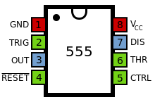
The connection of the pins for a DIP package is as follows:
| Pin | Designation | Description |
| 1 | GND | Ground reference voltage, low level (0 V) |
| 2 | TRIG | The OUT pin goes high and a timing interval starts when this input falls below 1/2 of CTRL voltage (hence TRIG is typically 1/3 V CC , CTRL being 2/3 V CC by default, if CTRL is left open). |
| 3 | OUT | This output is driven to approximately 1.7 V below + V CC or GND. |
| 4 | RESET | A timing interval may be reset by driving this input to GND, but the timing does not begin again until RESET rises above approximately 0.7 volts. Overrides TRIG which overrides THR. |
| 5 | CTRL | Provides "control" access to the internal voltage divider (by default, 2/3 V CC ). |
| 6 | THR | The timing (OUT high) interval ends when the voltage at THR is greater than that at CTRL (2/3 V CC if CTRL is open). |
| 7 | DIS | Open collector output which may discharge a capacitor between intervals. In phase with output. |
| 8 | V CC | Positive supply voltage, which is usually between 3 and 15 V depending on the variation. |
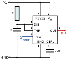
Pin 5 is also sometimes called the CONTROL VOLTAGE pin. By applying a voltage to the CONTROL VOLTAGE input one can alter the timing characteristics of the device. In most applications, the CONTROL VOLTAGE input is not used. It is usual to connect a 10 nF capacitor between pin 5 and 0 V to prevent interference. The CONTROL VOLTAGE input can be used to build an astable multivibrator with a frequency modulated output.

